- 您现在的位置:买卖IC网 > Sheet目录362800 > EVAL-AD5381EB (Analog Devices, Inc.) 40-Channel, 3 V/5 V, Single-Supply, 12-Bit, Voltage Output DAC
AD5381
TIMING CHARACTERISTICS
SERIAL INTERFACE TIMING
Table 6. DV
DD
= 2.7 V to 5.5 V; AV
DD
= 4.5 V to 5.5 V or 2.7 V to 3.6 V; AGND = DGND = 0 V; all specifications
T
MIN
to T
MAX
, unless otherwise noted
Parameter
1
,
2
,
3
Limit at T
MIN
, T
MAX
Unit
t
1
33
ns min
t
2
13
ns min
t
3
13
ns min
t
4
13
ns min
t
5
4
13
ns min
t
6
4
33
ns min
t
7
10
ns min
t
7A
50
ns min
t
8
5
ns min
t
9
4.5
ns min
t
104
30
ns max
t
11
670
ns max
t
124
20
ns min
t
13
20
ns min
t
14
100
ns max
t
15
0
ns min
t
16
100
ns min
t
17
8
μs typ
t
18
20
ns min
t
19
12
μs max
t
205
20
ns max
t
215
5
ns min
t
225
8
ns min
t
23
20
ns min
Rev. A | Page 8 of 36
Description
SCLK cycle time
SCLK high time
SCLK low time
SYNC falling edge to SCLK falling edge setup time
24
th
SCLK falling edge to SYNC falling edge
Minimum SYNC low time
Minimum SYNC high time
Minimum SYNC high time in Readback mode
Data setup time
Data hold time
24
th
SCLK falling edge to BUSY falling edge
BUSY pulse width low (single channel update)
24th SCLK falling edge to LDAC falling edge
LDAC pulse width low
BUSY rising edge to DAC output response time
BUSY rising edge to LDAC falling edge
LDAC falling edge to DAC output response time
DAC output settling time
CLR pulse width low
CLR pulse activation time
SCLK rising edge to SDO valid
SCLK falling edge to SYNC rising edge
SYNC rising edge to SCLK rising edge
SYNC rising edge to LDAC falling edge
1
Guaranteed by design and characterization, not production tested.
2
All input signals are specified with t
r
= t
f
= 5 ns (10% to 90% of V
CC
) and are timed from a voltage level of 1.2 V.
3
See
Figur
,
, and
.
Figure 2,
e 3 Figure 4
Figure 5
4
Standalone mode only.
5
Daisy-chain mode only.
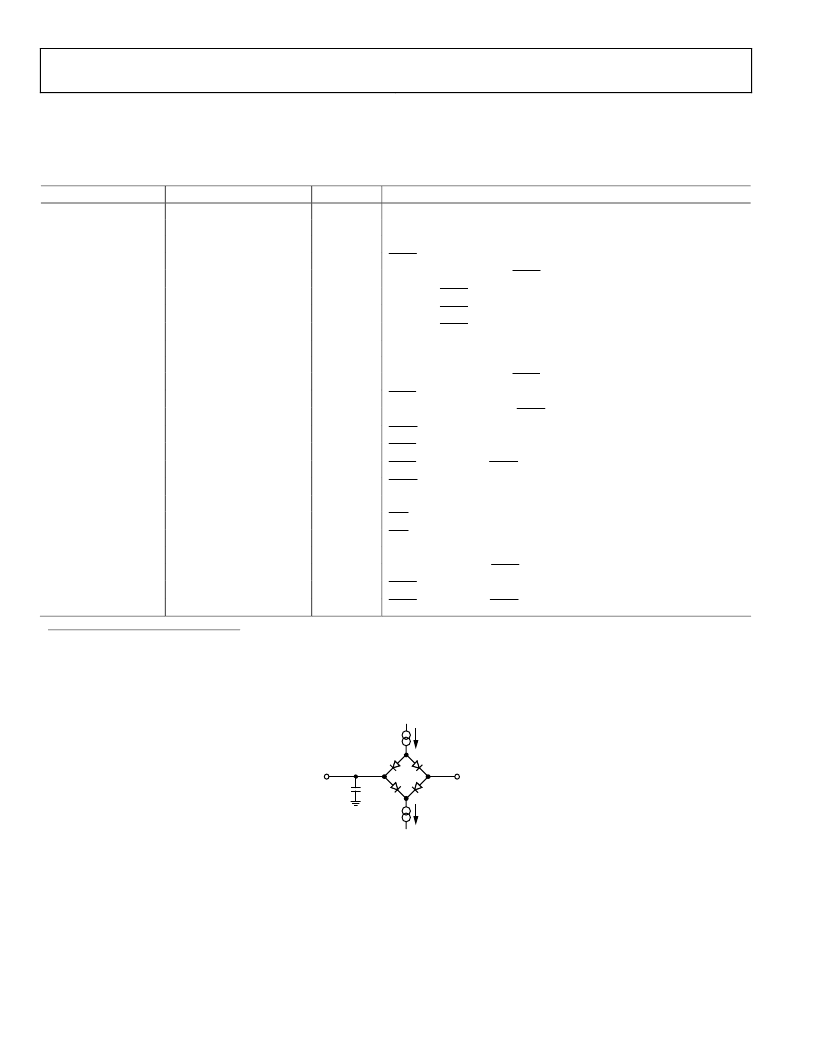
C
50pF
TO OUTPUT PIN
V
OH
(MIN) OR
V
OL
(MAX)
200
μ
A
200
μ
A
I
OL
I
OH
0
Figure 2. Load Circuit for Digital Output Timing
发布紧急采购,3分钟左右您将得到回复。
相关PDF资料
EVAL-AD5382EB
32-Channel, 3 V/5 V, Single-Supply, 14-Bit, Voltage Output DAC
EVAL-AD5383EB
32-Channel, 3 V/5 V, Single-Supply, 12-Bit, Voltage Output DAC
EVAL-AD5398EB
120 mA, Current Sinking, 10-Bit, I2C DAC
EVAL-AD5415EB
Dual 12-Bit, High Bandwidth, Multiplying DAC with 4-Quadrant Resistors and Serial Interface
EVAL-AD5426EB
8-/10-/12-Bit High Bandwidth Multiplying DACs with Serial Interface
EVAL-AD5432EB
CAP, .22UF, 10V, SMT, 0603
EVAL-AD5443EB
CAP X7R 470PF 50V 10% 0603
EVAL-AD5520EB
Per Pin Parametric Measurement Unit/Source Measure Unit
相关代理商/技术参数
EVAL-AD5382EB
制造商:Analog Devices 功能描述:EVALUATION BOARD I.C. - Bulk 制造商:Rochester Electronics LLC 功能描述:
EVAL-AD5382EBZ
功能描述:BOARD EVAL FOR AD5382 RoHS:是 类别:编程器,开发系统 >> 评估板 - 数模转换器 (DAC) 系列:- 产品培训模块:Lead (SnPb) Finish for COTS
Obsolescence Mitigation Program 标准包装:1 系列:- DAC 的数量:4 位数:12 采样率(每秒):- 数据接口:串行,SPI? 设置时间:3µs DAC 型:电流/电压 工作温度:-40°C ~ 85°C 已供物品:板 已用 IC / 零件:MAX5581
EVAL-AD5383EB
制造商:Analog Devices 功能描述:EVAL KIT FOR 32CH, 3V/5 V, SGL-SUPPLY, 12-BIT, VOLT OUTPUT D - Bulk 制造商:Rochester Electronics LLC 功能描述:
EVAL-AD5390EB
制造商:Analog Devices 功能描述:
EVAL-AD5390EBZ
功能描述:BOARD EVALUATION FOR AD5390 RoHS:是 类别:编程器,开发系统 >> 评估板 - 数模转换器 (DAC) 系列:- 产品培训模块:Lead (SnPb) Finish for COTS
Obsolescence Mitigation Program 标准包装:1 系列:- DAC 的数量:4 位数:12 采样率(每秒):- 数据接口:串行,SPI? 设置时间:3µs DAC 型:电流/电压 工作温度:-40°C ~ 85°C 已供物品:板 已用 IC / 零件:MAX5581
EVAL-AD5391EB
制造商:Analog Devices 功能描述:EVALUATION BOARD I.C. - Bulk 制造商:Rochester Electronics LLC 功能描述:
EVAL-AD5391EBZ
功能描述:BOARD EVALUATION FOR AD5391 RoHS:是 类别:编程器,开发系统 >> 评估板 - 数模转换器 (DAC) 系列:- 产品培训模块:Lead (SnPb) Finish for COTS
Obsolescence Mitigation Program 标准包装:1 系列:- DAC 的数量:4 位数:12 采样率(每秒):- 数据接口:串行,SPI? 设置时间:3µs DAC 型:电流/电压 工作温度:-40°C ~ 85°C 已供物品:板 已用 IC / 零件:MAX5581
EVAL-AD5392EB
制造商:Analog Devices 功能描述:EVAL BD FOR 8-/16CH, 3V/5 V, SERL INPUT, SGL-SUPPLY,12-/14BI - Bulk